Optical ReceiversOptical receivers have the following parts:
- photodetector – converts received optical power to current - preamplifier – amplifies electrical signal - receiver filter – filters electrical signal to reduce the noise - signal processing circuits – demodulator, retiming and clock signal extraction Receiver Block Diagram 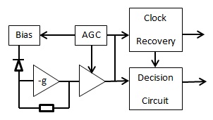
Photodetectors Characteristics of a good photodetector are: - sensitivity over the required band - efficiency - fast response time - low noise - small size - high reliability - low cost How Photodiodes Work? A photon with energy greater than band gap energy of the semiconductor (Eg), is absorbed to generate and electron hole pair which results in electric current. Photo energy equals to hf where h is Planck’s constant (6.626*10^-34 Js) and f is frequency. If hf < Eg then absorption is zero. Wavelength which results in band gap energy is referred to as the band edge wavelength. It equals to: 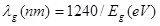
Typical band edge wavelength for well-known semiconductor materials:
- Silicon (Si): 1090 nm - Germanium (Ge): 1850 nm - Gallium Arsenide (GaAs): 870 nm - Indium Gallium Arsenide (InGaAs): 1680 nm Optic fibre systems which operate at 1300-1600 nm thus use InGaAs. Photodiodes operate in reverse bias because reverse bias increases the depletion area of p-n junction and thus: - increases sensitivity, - decreases capacitance There is leakage current even when there is no light. It is called dark current. Photodetector Parameters Photodetector has two parameters: quantum efficiency and responsivity. Quantum efficiency is the probability that a photon will create an electron hole pair. It is dependent on absorption coefficient of the material and detector shape. It is defined by: 
Reponsivity is defined the ratio between produced photo current and incident optical power. The unit is amps per watt. It equals to:
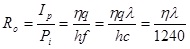
The wavelength if defined in nm.
One way to increase quantum efficiency is to increase the width of depletion region. A lightly doped intrinsic semiconductor is placed between p-type and n-type semiconductor regions to create PIN photodiode. Generated electrons and holes are also referred to as photo carriers. Shot Noise The generation of current is a random process because different amount of photon arrive at different times. Thus noise exits. It is known as shot noise which limits the sensitivity of the photodiode. It is given by: 
Where: I = Ip + Id, Ip = Photodiode current, Id = Dark current
q = Electric charge = 1.6 * 10^-19 C B = Filtered noise bandwidth Thermal Noise
Thermal noise increases with rise in temperatures: 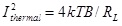
Where: k = Boltzmann’s Constant = 1.38 * 10^-23 J/K
T = Temperature in Kelvin B = Bandwidth in Hz RL = Load Resistance in ohms Relative Intensity Noise (RIN)
Relative intensity noise is given by: 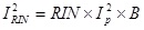
Where: Ip = Current generated from incident photons,
RIN = Constant Total Noise
Total Noise equals to the addition of noise sources: 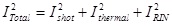
Avalanche Photodiodes In Avalanche Photodiode (APD) electric field is used to provide photo carriers with more kinetic energy. The electric field is created on edge of intrinsic region. Collisions between energetic carriers and crystal lattice result in electron holes. The free electron which creates the hole can cause more ionisation also known as impact ionisation thus leading to avalanche multiplication. The equation for shot noise in APDs equals to: 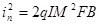
Where: M = APD gain,

Therefore:
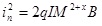
x is 0.3 to 0.5 for silicon APDs and 0.7 to 1 for germanium and InGaAs APDs.
Frequency Response The frequency response of a photodiode is limited by photodiode capacitance and load resistance. The value capacitance increases with the size of active area and reverse bias voltage. The active area diameter of high speed photodiodes is 30 to 200 micro-meters. Preamplifiers A photo detector can be sold with inbuilt preamplifier that is made from bipolar junction (BJT) or field effect transistors (FET). |
